Scope:
Often when a person approaches the process of product development, he only has a faint notion of the development process, how long will it take? What will be the cost? What are the risks etc.
In this article I try to clear some of the ambiguity, and provide an outline description to the process.
A hardware product is a very broad term and branches to many types of design, in this article I try to describe the common steps to all hardware design, with slight focus on consumer type hardware.
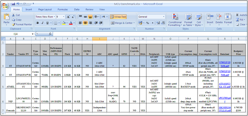
Product cycle summary
Table below summarizes the stages of the hardware development.
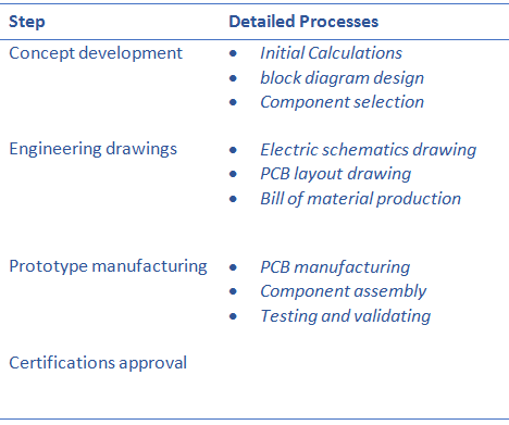
Concept Development
Initial Calculations
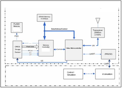
The foundations of any development start with translating the client’s idea into an engineering structure. As a general example, consider a request for a device attached to a dog collar transmitting the dog’s whereabouts. It is the engineer’s job to figure out:
- What will be the transmitter (Bluetooth? WIFI? …)
- What is the battery type?
- What will be the transmission power, and how will it affect the battery life?
- What is the data transmitted, how “large is it? Is it stored on the dog’s collar?
These are just the very basic questions that need to be researched, defined and calculated, in order to formulate a clear engineering structure.

Component Selection
Once the engineering structure is done, the next step is to select the appropriate components (or ICs) for the product. There are many components vendors that offer a wide variety of components.
The selection is done according to various considerations such as: electric compatibility, performance, cost, purchase lead time, production ease etc.….
Consider the importance of this stage: for instance, if you choose a simple component that is 10 Cents higher priced, when reaching mass production and manufacturing 10,000 pieces, it will cost a $1000 more!
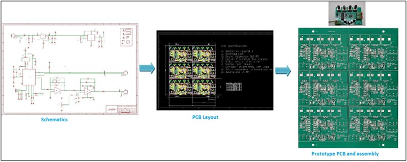
Engineering drawings
The engineering drawing are the translation of the “concept design” into the “real world”, i.e. with these drawings manufacturer will be able to produce the actual product.
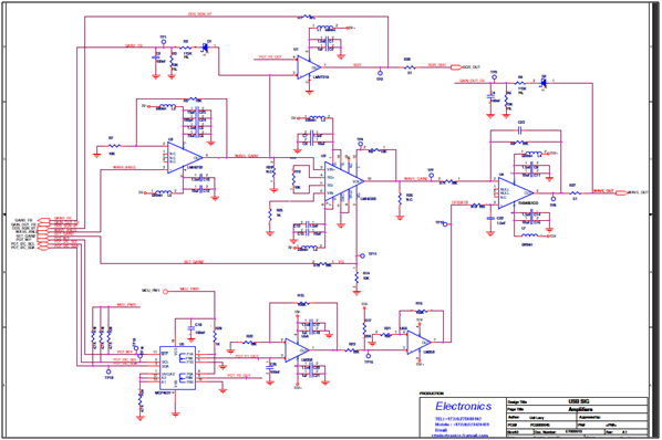
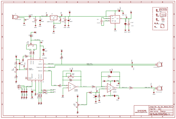
Electrical Schematics Drawing
The electrical schematics is the “logical connection” between all the components of the hardware product, the electronics schematics should be designed with special care considering all strict electrical rules, power considerations, electronics phenomenon such as RF noise, manufacturers recommendations etc…
It is also important to draw clear and comprehensible drawings, so that any engineer in the future will be able to pick up this schematic and continue it.
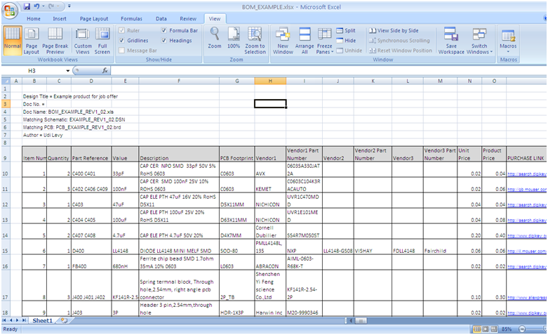
Bill of materials (BOM) production
One of the products of the electrical schematics is the BOM file (bill of materials), it is an excel file containing a list of all the components on the hardware product.
This file is very important, as it will be used for purchasing the materials for the project. A mistake in this file can be fatal when reaching mass production – each component in this file will be purchased by the thousands, therefore it is critical that it is accurate.
Therefore, it is very important to have a BOM that was verified component by component, includes all information for manufacturing, exact manufacturers part number and comprehensive file name linked to a specific schematic.
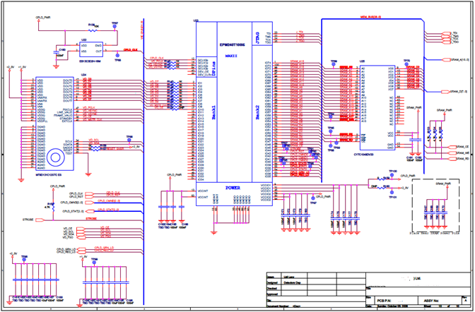
PCB Layout drawings
Once the electrical schematics is done, the next step is the PCB (printed circuit board) layout. The PCB is the actual electrical board that contains all the electrical connections between the components or ICs.
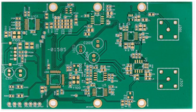
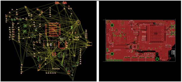
The process of laying out the PCB is done using a CAD software that allows drawing the actual electrical connections between the components.
Below is a screen shot of the CAD software. On the left is a picture at the start of the layout, the yellow lines indicate the connection between the components.On the right is the picture at the end of the process after all components have been placed and proper electrical connections between the components are drawn.
Prototype manufacture and testing
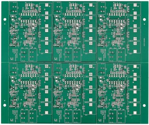
PCB Fabrication and assembly
Using the files produced from the CAD software (known as gerber files) are send to PCB manufacturers to be fabricated. PCB prices can range from 1$ to 1000$ (or even more in extreme cases), depending on the size, material and complexity of the PCB.
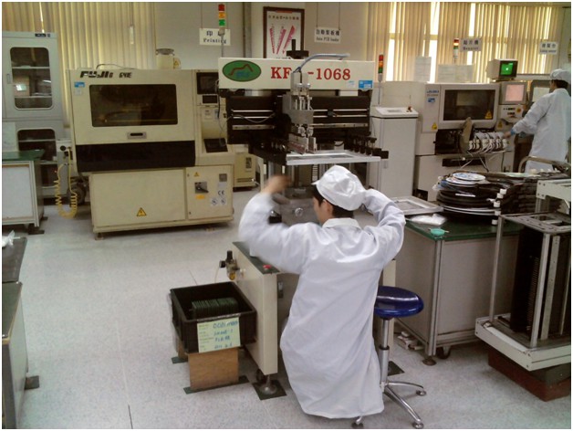
Component assembly
After the bare PCB arrives it is necessary to assemble the components on it.
Component are either hand assembled using solder iron, or sent to machine assembly in factory, depending on the complexity and the number of required units.
In very small quantities hand assembly will be quicker and cheaper, but as the quantity increases it is better to use machine assembly.
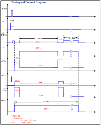
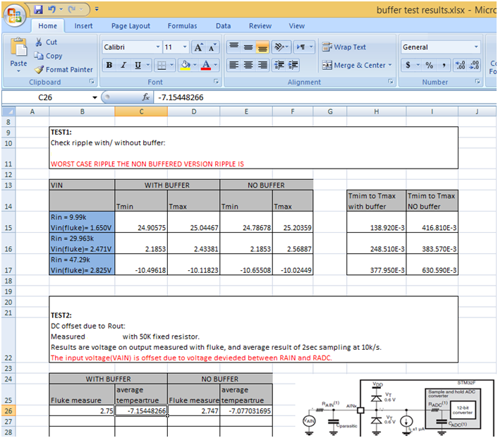
Circuit bring-up Tests
After the board components are assembled, it must be tested to verify there are no mistakes in the design, only after thorough electrical test (usually called “bring-up”) the product can be released. For example, see below analog circuit test report.
Concept Development
The last step before a product can be mass produced is certification approval.
In order to sell or export a product into a country, the product must pass certain tests insuring that it is safe and complies with the country’s electrical requirements.
To insure this each country requires that the product pass defined set of tests. The tests defer from country to country, while USA uses a set of tests defined by FCC (Federal Communications Commission) in Europe CE (European Conformity) certifications are used, and there are numerous other certification bodies for other countries.
The certification process is costly and also has a long duration, weeks or months, depending on the complexity of the product.
Summary
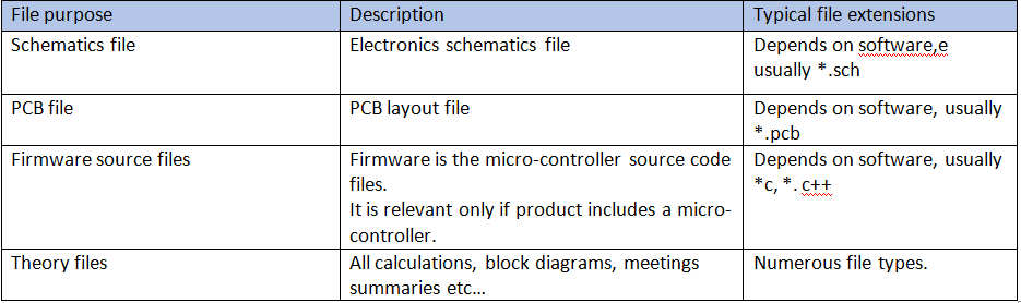
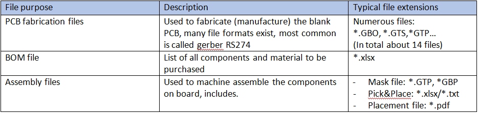
To summarize, the product of all stages described above is a set of files called “production file”.
The production file is a set of files that allows manufacturers to manufacture the product, and include the following files:
In addition to the production file, it is important to have the “raw material”, that is the set of files that allow to modify the product if needed, typically includes the following files: